How to use the Atari ST hard disk port
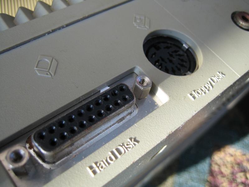
When I set about to interface to the Hard Disk Port on my Atari 1040ST I assembled all the documentation I could find and discovered that, though I found plenty, I still ended up without quite enough to design the interface. I attacked the problem with the Scientific Method and now have a working one-megabyte-per-second interface. This article was written to give others the information that I needed in hopes that they will not be frightened of using what has turned out to be a very simple and easy-to-use port.
Since much of the information in this article is based on experiment with only one DMA chip it is possible that some of it will not apply to other revisions of the chip. Perhaps someone at Atari will correct any misconceptions or outright errors. Also, the interface I built only does DMA transfers into the ST (read operations); therefore, while it is easy to infer the appropriate protocol, I haven't tested DMA transfers in the opposite direction.
DMA IN THE ST
The same DMA channel is used for both the floppy disks and the Hard Disk Port. The floppies are controlled by a floppy disk controller chip which is connected to the DMA chip. The DMA chip is capable of servicing data requests at about 1.25 MHz. If you attempt to transfer data at a rate greater than that data will be lost. I have been able to transfer data at very close to this rate without any problems. The DMA chips buffers 16 bytes of data before requesting the memory buss then holds the buss until all buffered data has been transfered. Memory cycles used for DMA are taken from the processor; since the memory buss makes 4 MByte/s available, 1 MByte/s of DMA should take 25% of the cycles normally available to the processor, plus a fudge factor to account for the time spent in arbitration.
THE HARD DISK PORT
The Hard Disk Port is a 19-pin D connector - apparently completely unavailable through normal commercial channels. I made my own from a metal-shelled male DB25 connector as follows:
- remove and discard the metal shell revealing that the pins are held in place and insulated with two loose plastic retainers;
- remove the pins from the retainers (for once you can lose a couple since you will end up with six spares);
- using a fretsaw or a fine hacksaw remove one end of both retainers leaving 19 holes;
- replace the pins and glue the retainers together.
You now have the connector you need. It has no mounting ears but the retaining force of 19 pins is quite substantial. If this is not adequate you could perhaps ingeniously salvage the metal shell somehow.
The pins on the Hard Disk Port are connected as follows (pin one is at the upper right of the connector facing the rear of the computer):
- 1-8 DMA data buss bits 0-7 (bidirectional)
- 9 Hard Disk Controller Chip Select (_HDCS) (output)
- 10 Interrupt Request (_IRQ) (input, internal 1k pull-up)
- 11 Ground
- 12 Reset (bidirectional)
- 13 Ground
- 14 Acknowledge (_ACK) (output)
- 15 Ground
- 16 A1 (output)
- 17 Ground
- 18 Read/_Write (R/_W) (output)
- 19 Data Request (_DRQ) (input, internal 1k pull-up)
The Hard Disk Port is connected directly to the DMA chip WITHOUT ANY BUFFERING on most pins - be careful, a small mistake (e.g., static) could blow your DMA chip. The system reset line is also directly connected to the port meaning that accidental shorts reset your computer - very irritating.
INSIDE THE DMA CHIP
The DMA chip is accessed through memory-mapped registers:
- ff8604 R/W 16 bits
- When bit 4 of the Mode register is zero a read or write access to this word causes a read or write cycle on the DMA buss. If bit 3 is set the Hard Disk Chip Select controls the cycle; otherwise, the Floppy Disk Controller is selected. R/_W is set according to the type of the CPU access and A1 is set according to bit 1 of the Mode register. NOTA BENE: what is called A0 in the DMA chip is called A1 on the Hard Disk Port. For some reason, if bit 7 is not set no DMA buss cycle will take place.
- When bit 4 of the Mode register is one the internal sector count register is selected. This register counts down the number of 512-byte blocks that have been transferred. When the sector count register reaches zero the chip will cease to transfer data.
- ff8606 R 16 bits Status word:
- bit 0: 1 if error.
- bit 1: 1 if sector count is zero.
- bit 2: 1 if _DRQ is active.
- If this word is polled during a DMA operation the transfer will be disrupted. End of transfer must be signalled with the _IRQ signal. The status is cleared by toggling bit 8 in the Mode register.
- ff8606 W 16 bits Mode register:
- bit 0: not used.
- bit 1: A0; state of Hard Disk Port line A1 (sic) during a DMA buss cycle.
- bit 2: A1; used for Floppy Controller only.
- bit 3: HDC/_FDC chip select; if this bit is 1 the _HDCS chip select will be generated; otherwise the Floppy Controller select.
- bit 4: If one, select the the internal sector count register for access at ff8604.
- bit 5: Reserved; set to zero.
- bit 6: Disable DMA when set; this is not used by Atari.
- bit 7: FDC/_HDC transfer select; if set DRQ from the Floppy Controller is acknowledged; otherwise, DRQ from the Hard Disk Port. This bit must also be set to get a DMA buss cycle for some reason.
- bit 8: Write/_Read; if set, data will be transferred out of memory; otherwise, into. Toggling this bit also clears the DMA chip status.
- ff8609 R/W 8 bits DMA Address Counter High byte.
- ff860b R/W 8 bits DMA Address Counter Mid byte.
- ff860d R/W 8 bits DMA Address Counter Low byte.
- The DMA Address Counter must be loaded in Low, Mid, High order.
There are two eight-word FIFOs in the chip; one for buffering read operations and one for writes. The FIFOs are not flushed automatically so you can only transfer data in multiples of 16 bytes. Actually, use 512-byte units like the sector count register does.
The DMA chip has no interrupt capability; This is ickky, but cheap. End-of-transfer interrupts must be generated by the external controller and are masked and vectored by the 68901 MFP chip on the General Purpose I/O Port, bit 5, interrupt level 7. The MFP chip interrupts are controlled with the XBIOS calls 'mfpinit', 'jdisint', and 'jenabint'. 'jenabint(7)' and 'jdisint(7)' will enable and disable the DMA interrupt. 'mfpint(7,dmahandler)' will initialize the vector to 'dmahandler', wiping out any earlier one. If you want instead to simply test the state of the interrupt request line, without taking any interrupts you can test the MFP GPIP data register. Read a byte from fffa01 and mask with $20; if the result is zero there is no interrupt.
Because the floppy controller shares the DMA chip you have to be very careful about two things: 1) do not leave DMA interrupts enabled accidentally or floppy operations will call your DMA interrupt handler; 2) turn off the floppy check routine while using DMA by jamming a 1 into FLOCK=$43e to prevent this periodic operation from screwing up your transfers by altering the DMA chip registers.
TIMING
These timing contraints are my interpretation of sketchy, preliminary-looking Atari documents dated "27 September 1985". If someone at Atari can give better figures, please inform me.
There are two separate types of transfer on the DMA buss: processor cycles, which are initiated by the processor, and DMA cycles, which are initiated by the external controller. The processor initiates a DMA transfer by waking up the controller with a few command bytes then gives it control of the DMA buss. The controller then uses the DMA buss as long as it needs it and returns control by interrupting the processor.
Processor cycles are controlled by the _HDCS, R/_W, and A1 lines in the usual fashion. On a write cycle, the DMA chip gives you 60 ns of setup on A1, data, and R/_W before asserting _HDCS for about 250 ns, then holds for no more than 20 ns. On a read cycle, you get the same setup for A1 and R/_W, and you must give the DMA chip 100 ns setup oe data before _HDCS is retracted. Hold time should be less than 80 ns.
Data cycles are initiated by the external controller by asserting _DRQ. _ACK will be asserted by the DMA chip no more than 240 ns later. _DRQ may then be retracted. _ACK is asserted for about 250 ns. In a read operation (data from controller to memory) data should be setup 60(?) ns before _ACK is retracted and held for 50(?) ns. In a write operation (data from memory to controller) data is valid 60 ns before _ACK is asserted until 60 ns after _ACK is retracted. _DRQ for the next cycle may not be asserted earlier than 240 ns after _ACK has been retracted.
INTERFACING IT
This interface transfers a byte into the the DMA chip whenever a rising edge is seen on the data strobe input. This interface cannot coexist with a hard disk because it will respond to commands intended for the hard disk. Bear with me, we'll tackle that later.
Rather than attempt to render several schematics in ASCII I will describe the circuits and let you draw the schematics. If the instructions don't make any sense you probably should not attempt to make the interface. It's all very simple if you know exactly what you are doing; if you don't - you're dead.
A SIMPLE, READ/WRITE INTERFACE
If all you want to do is read and write bytes it is very simple: You simply use the Chip Select, R/_W, and A1 lines to select two write registers and two read registers. If you need more than that all you have to do is use A1=0 to select an address register which selects the register you get on a cycle with A1=1. One thing that you have to consider is that the ST writes to the Hard Disk Port several times during its booting procedure, presumably to determine if there are any hard disks connected. Apparently, if no interrupt is received in response to these writes the ROM assumes that no controller is connected.
In my interface there is a mode register which is accessed when A1=0. It has two control bits and two bits connected to a decoder which determines which of three other registers are selected when A1=1.
ADDING AN INTERRUPT
If an interrupt is needed (probably why you want to use this port) you need a flipflop to store the interrupt state and some way to reset it. I used a 74LS74 for the flipflop with a diode on the output to get the open-collector action. This diode is not needed if there is no other device on the Hard Disk Port. (But don't scrimp on a diode...) I reset the interrupt with any access to the mode register but other methods would work as well. Make sure that the circuit will always leave reset with the interrupt cleared. I arranged this by having a circuit enable bit in the Mode register, which is cleared by system reset. If you screw up on this your floppy will not work because the same interrupt is used for both floppy and hard disk controllers. I learned a little about the file system the hard way while debugging this interface - I recommend getting the interrupt reset system right the first time.
ADDING DMA
Once you can write to your mode register adding DMA transfers (at least for read operations) is very simple. All you need is another flipflop to do the Data Request synchronization and a 3-state octal latch (74LS374) to hold the data. Connect the output to the DRQ line with a diode as with the interrupt flipflop. When data is available clock it into the data register and clock a zero into the flipflop. This generates a data request for the DMA chip. When it gets around to it the DMA chip will assert _ACK, which means it is ready to accept the data. Since you have the _ACK signal connected to the three-state enable pin on the data register the data is driven onto the buss. You also use the _ACK signal to set the flipflop. When the DMA chip no longer needs the data it will retract _ACK and you can begin another transfer. Spurious data requests are not as nasty as spurious interrupts because the DMA chip does not listen to hard disk data requests if it is listening to the floppy disk controller. Naturally, if there is a real hard disk out there, there had better not be any spurious data requests.
CO-EXISTING WITH A HARD DISK
I do not own a hard disk; therefore, the suggestions in this section are totally untested.
The Atari-defined protocol allows seven (eight) different controllers on the DMA buss. In order to make an interface which will not interfere with other controllers you must understand the protocol. Each command is initiated with a processor write cycle which sends out a Command Byte (A1=0) on the DMA buss. The most-significant three bits contain the controller number and the remaining bits contain an operation code. The controller whose number matches the controller number in the Command Byte responds to the operation code. Some operations require parameters, which are sent as Data Bytes (A1=1) following the Command Byte. The controller generates an interrupt after coping with each byte. After the last Data Byte is sent the controller takes over the buss for the DMA transfer. When the transfer is finished the controller generates an interrupt.
In order to keep out of the way of other controllers on the buss it should only be necessary to select your interface with a Command Byte with the proper format. After that use data bytes as you wish, since all other controllers will not be selected.
GOOD LUCK!
Using this information anyone with any experience in interfacing can produce a working DMA interface. Best of luck and drop me a line if you find this useful.
--
Doug Collinge
School of Music, University of Victoria,
PO Box 1700, Victoria, B.C., Canada, V8W 2Y2
collinge@uvunix.BITNET
decvax!uw-beaver!uvicctr!collinge
ubc-vision!uvicctr!collinge


